Table Of Content
There's been quite a lot of speculation in the market about the possibility of a transformative deal being done. I guess, given that we have you on the mic here, maybe if you get a sense from yourself, what would be the sort of thing that a business like Cadence could look for? Could that be the sort of ambition that Cadence would have given the silicon to systems opportunities that are emerging? I mean, we are proud to have a very strong partnership with Arm and with our joint customers, Arm and Cadence customers. I think we have had a very strong partnership over the last 10 years, I would like to say, and it's getting better and better.
Why it’s so hard for China’s chip industry to become self-sufficient
Not only do smart products such as mobile phones and computers contain chips, it can be said that as long as some more complex functions are involved, they will be used. Without the advent of chips, it would be hard for us to imagine what the current electronic age would be like. It is precisely because of the invention of the chip that all functions are concentrated in a small chip.

Personal tools
We had strong growth at hyperscalers, and over 50 customers have deployed our digital solutions on three nanometer and below design. Cadence Cerebrus, which leverages Gen.AI to intelligently optimize the digital full flow in a fully automatic manner now has been used in well over 350 tapeouts. Samsung used Celsius Studio to uncover early design and analysis insights to precise and rapid thermal simulation for 2.5D and 3D packages, attaining up to a 30% improvement in product development time. And a leading Asian mobile chip company use optimality intelligence system explorer AI technology and Clarity 3D Solver obtaining more than 20 times design productivity improvement. We announced a collaboration with Arm to develop a chiplet-based reference design and software development platform to accelerate software-defined vehicle innovation.
Detailed Introduction of the Chip Design Process
One of the things I would say is, use the tools that are available. There’s a vast community of people working on these things, and you can find lots of examples [of applications and techniques] on GitHub or MATLAB Central, where people have shared nice examples, even little apps they’ve created. I think many of us are buried in data and just not sure what to do with it, so definitely take advantage of what’s already out there in the community. You can explore and see what makes sense to you, and bring in that balance of domain knowledge and the insight you get from the tools and AI. Both chip design and manufacturing are system intensive; you have to consider every little part. It’s a case where you might have models to predict something and different parts of it, but you still need to bring it all together.
Step 2: Architecture / system design
Although the phases are presented here in a straightforward fashion, in reality there is iteration and these steps may occur multiple times. I think what you're getting at there is what we would call add-ons. Typically, we have the very predictable software renewal business. And you'll see in the recurring revenue part of our business, I think we're at double digit revenue growth. But over the past few years, I think that's been at low teens.
OpenLane 2 boost for custom open source chip design ... - eeNews Europe
OpenLane 2 boost for custom open source chip design ....
Posted: Tue, 23 Apr 2024 15:32:55 GMT [source]
That’s all about to change thanks to the popular open standard known as RISC-V. Right now, at top research institutions such as the University of Michigan, it would be nearly impossible to mimic the highly complex design work that goes into their state-of-the-art chips. Such institutions are also more likely to be able to pay the high cost of fabrication to test the viability of their designs in an actual prototype. Reinforcement learning is suited to electronic design automation (EDA) workloads based on its ability to holistically analyze complex problems, solving them with the speed that humans alone would be incapable of.
Step 4: Verification
But overall, the AI and hyperscalers, they are doing a lot more than so are the big semi company. Yeah, we try to derisk the guide -- with the assumption that there is going to be strong demand for the newer systems. But it will give us the opportunity to put some of the older systems into the cloud because we have a large underserved community that want to use our emulation capacity. But we haven't had a lot of capacity to share with them through our cloud offering. To the extent we do that, that will lead to ratable revenue though, because I think when it is used in the cloud, you get revenue over time, whereas when we deliver and they use it on-prem, we take revenue upfront. That means not just hyperscalers, but perhaps in AI PCs and beyond.
RTL design
Chips developed from these design kits are now also invited to be fabricated at no cost to the developer thanks to a cooperative research agreement between the U.S. Department of Commerce’s National Institute of Standards and Technology (NIST) and Google. Using logic restructuring for the areas to be timing met, Use the useful skew , if permissible by meeting the hold-time requirements.
This process of chip design involves the knowledge of circuit design and its logic formation. All chips are made using basic elements which are known as transistors. The Metal Oxide Silicon Field Effect Transistor (MOSFET) is the basic building block of digital chips which is used to make complex circuits. The future of chip design is exciting and rapidly evolving, as technology advances. Next-gen chipsets enable new-age solutions by offering higher performance, lower power consumption, and increased functionality. These advancements drive innovation across many industries.
Now in terms of BETA, it made sense because it is a very good technology. And we are focused on finishing that acquisition, and also integrating that -- that will take some time. I just wonder whether that's part of the reason that's weighing on your Q2. I understand you mentioned that you're going through that second-gen to third-gen hardware transition right now.
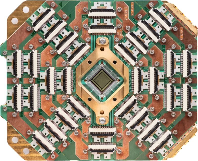
As the challenges grow, so must the hardware used to emulate and debug the chip and prepare the software that will run on the semiconductor once it is back from the fab. In isolation, this ranks as a small effort from Microsoft to make a foray into the world of chips. Nevertheless, Fungible could eventually play a pivotal role in the data center industry (which is the basic computing unit of cloud computing, data, and apps housed in a remote data center and accessed via internet connection). At this time, the chip to be tested has been wrapped in a layer of packaging and is not so fragile. Therefore, the requirements for the test environment are not so strict, and there is no need for cleanroom testing. However, for packaging testing, due to the obstruction of the package itself, the test probe cannot touch the inside of the chip, and the test range is limited, and the complexity of the test is also increased.
"When I was designing chips myself, I never did it. But I think it's something that if it had occurred to me, I probably would have done it, just for fun." The software is fully customizable according to the user’s needs. The pro version of Gravit is paid and has more advanced features like advanced export options, offline version, more color space, etc.
Standard cells are usually placed following standard cell rows. Our IP business continued to benefit from market opportunities offered by AI and multi-chiplet based architecture. We are seeing strong momentum in interface IPs that are essential to AI use cases, especially HBM, DDR, UCIe, and PCIe at leading edge nodes. In Q1, we partnered with Intel Foundry to provide design software and leading IP solutions at multiple Intel-advanced nodes. Over the past six years, we have methodically built out our system analysis portfolio. And with the signing of the definitive agreement to acquire BETA CAE, are now extending it to structural analysis, thereby unlocking a multi-billion dollar TAM opportunity.
For final testing, another important step is to add internal test nodes within the system which are critical to debug the system while testing on actual PCB. The next step is to design the architecture of the system where we decide which blocks are going to be used and what hierarchy level this system is going to operate. For practical reasons we will use in this article an example of a 4×4 Array Multiplier design which is a digital design. The United States faces a similar skills challenge, but with a twist. The United States is a global leader in advanced science and engineering research and education.


No comments:
Post a Comment